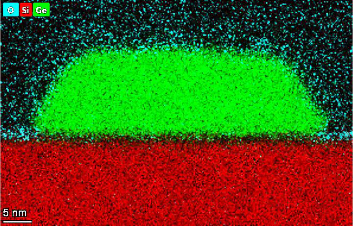
 EDX chemical characterization of the nanowires-substrate interface.
This work aims to investigate which are the best rapid thermal annealing (RTA) parameters for crystallizing Germanium nanowires grown on a patterned Silicon substrate, with the prospect of employing the nanowires as quantum dots for quantum computing applications (hole spin qubits). To this purpose, the features we are looking for are good quality and defects free crystal structure, and epitaxy with Silicon. Indeed, the presence of an epitaxial relation between Germanium and Silicon will lead to a hole mobility enhancement. There is a lattice mismatch of 4,2% between Si and Ge (since Ge has a greater lattice parameter with respect to Si) which induces a compressive strain in the Ge crystal structure when it is epitaxially grown on Si at room temperature. On the other hand, Ge features a larger thermal expansion coefficient so, after the annealing process (temperatures higher than 500°C), a reverse situation occurs: Ge undergoes tensile strain because it shrinks more when cooled down after annealing. The induced strain lifts valence band degeneracy (heavy hole and light hole bands are degenerate at gamma point in Germanium) reducing interband scattering with a consequent hole mobility enhancement. Ge nanowires could also relax this strain by forming misfit dislocations at the interfaces between the two materials. In this case we would lose the mobility enhancement effect induced by strain, thus we want to avoid the formation of defects at the interface. We also want to avoid the presence of Si intermixing, which could be induced by high temperature annealing, since it would be detrimental for quantum dots. Ordered array of nanowires have been fabricated on an e-beam patterned Si substrate by evaporation using the lift-off technique. They were successively crystallized, using the solid phase epitaxy approach (SPE), by rapid thermal annealing. This unconventional approach has been chosen because of the scalability: the possibility of mass production is fundamental since a large number of semiconductor qubits are required for quantum computing applications. In addition, evaporation allows to grow nanowires networks. This is extremely useful for quantum comput- ing since it provides a simple way to link different quantum dots obtaining qubits superposition. The nanowires have been then analyzed through Raman spectroscopy, scanning and transmission electron microscopy.
Read the full project report here.
Daniele Cucurachi
Computational Physicist
I am a computational physicist interested in a wide range of exciting problems ranging from machine learning to quantum computing. On the side, I collaborate with Scientifica VC, a venture capital firm specializing in deep tech startups.